CSS 422 - Intro to Hardware
Hardware Architecture
Introduction
Components are the processor, memory, IO... But the computer is organized to put these components together.
Organization handles the signals, interfaces, and peripherals between components.
Why Binary?
Tracking different voltages is really difficult, on and off is much easier. Further, switching numbers is very fast with binary.
How to convert any decimal into any base?
Cool algorithm. Divide the number by the base, the remainder is a digit in the new base. You keep dividing until the digit is less than the base, which is the first digit in your result. You order the numbers backwards because the first division is lke the first power, the second division is like the second power, and so on.
For example: 73,503 becomes 4,323 and a remainder of 12 (C). Then 254 remainder 5. Then 14 remainder 16 (G). Then finally
- 73,503
- 4,323 r12 (C)
- 254 r5
- 14 r16 (G)
- 0 r14 (E)
- EG5C
Logic
- IC (Integrated Circuit) Units consist of gates
- a Gate is an electronic circuit.
- Simple gates are combined to create complex functions.
Symbols
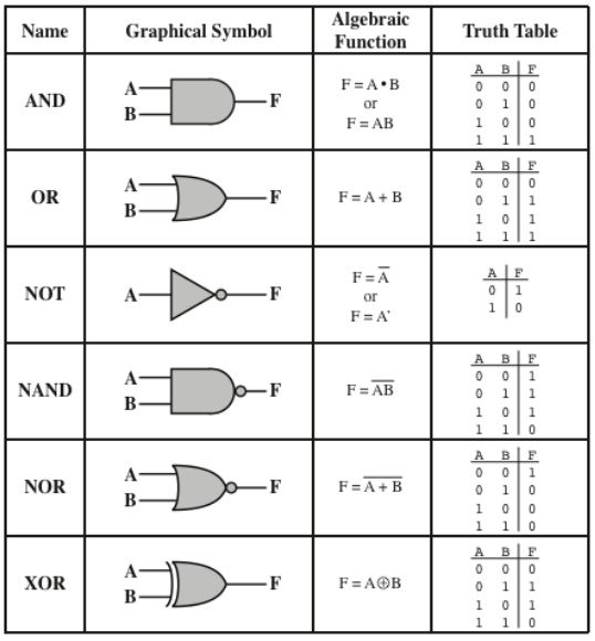
Positive and Negative Logic
- A logical operation has 2 different implementations
- These only concern the physical voltage outputs.
- Positive logic follows that 1s are high voltage.
- Negative logic follows that 1s are low voltage.
Designing a Digital System
- Given inputs and target outputs, build a circuit diagram to result in the outputs.
- Use the 3 gates: And, Or, & Not.
- Based on the purpose of the system, decide the number of inputs and the number of outputs needed.
- Figure out how many bits are needed for input and output.
- Draw a truth table for each input combination and output combination.
- How many combinations for 3 bits of input? Derive a boolean equation for each output.
- Connect inputs to outputs using logic gates
- Test if your circuit matches the design (truth table)
Karnaugh Maps
- A systematic method to derive a boolean equation from a truth table.
- For each output, build one K-map.
- Num of cells = num of possible combinations of input variables.
- 2n cells
- 3 Inputs (A, B, C) = 8 cells
- 4 → 16 cells
- The horizontal and vertical axes are labeled such that only one variable changes from complemented to un-complemented as you go across or down.
- The first and last cells in a row or column are considered adjacent.
- Place a 1 in the cells that output a 1, leave the other cells empty.
- Form the largest possible loops containing adjacent 1 entries of cells, as long as the loop is a size of 2.
- Each loop represents a part of the full term.
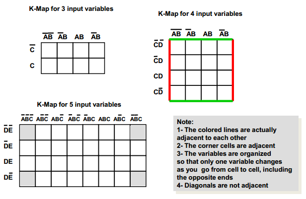
You can use K maps to determine not outputs too
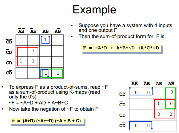
Notice the output is now a product of sums, instead of a sum of products. Just a flavor preference.
Combinational Circuits
What is a combinational circuit?
- Current output state depends only on input states.
- Basic building blocks of combinational circuits are logic gates.
- Combinational Circuits are called "memoryless circuits" because they don't store memory. Only care about current input.
Read Only Memory
- ROM is memory that is implemented with combinational circuits.
- A given input to the ROM (address line) always produces the same output (Data lines).
- Memory can only have 2n possible outputs, where n is the number of input bits.
- Memory can, however, output as many bits as it needs.
Applications
- MUX (Simple Multiplexer). Selects an input.
- Decoders are the opposite, given an input, only one of several outputs will be 1.
- Comparators.
- Arithmatic Circuits.
Arithmatic Logic Unit
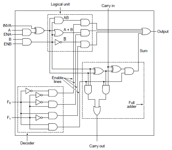
- Arithmatic Logic Units. 2 main inputs, A and B.
- The decoder only selects one logic operation for the inputs.
- The Logic Unit performs a logic operation
- The full adder adds.
- String 8 together to get an 8-bit ALU.
Sequential Circuits
- Circuits with memory.
- Current output depends on the current input, and the past history of i/o.
Latch
- Two inputs, one output. Either in a 0-state, or a 1-state.
- The circuit remains in its state until input is recived. It is latched.
- This persistent state is memory!
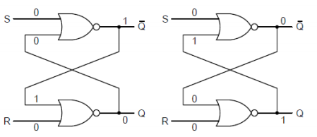
How
- Feedback, brings the output back as an input
- Locks the gate pair into a new state
- Set input sets the state to 1.
- Reset input sets the state to 0.
- S and R cannot be both 1. This is a race condition and breaks the circuit.
- SR is an asynchronous operation.
Synchronous Logic
- The clock is a digital analog of a pendulum.
- Duty Cycle is the amount of time the signal has a high-pulse.
- A square wave has a 50% duty cycle.
- Shorter high-pulse time has a lower duty cycle.
- As long as the pulse is greater than 2.5 volts, it's a 1. Below 1 is a 0. Inbetween is undefined.
- Propagation Delay is the time it takes from input change to output change.
- This limits unlimited clock speed.
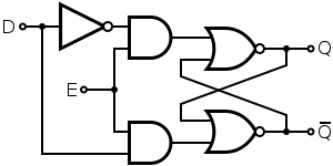
Flip-Flops
- The exact same as Latches, but have a clock input.
- The building blocks of sequential circuits.
- Only allows input when clock is active.
SR

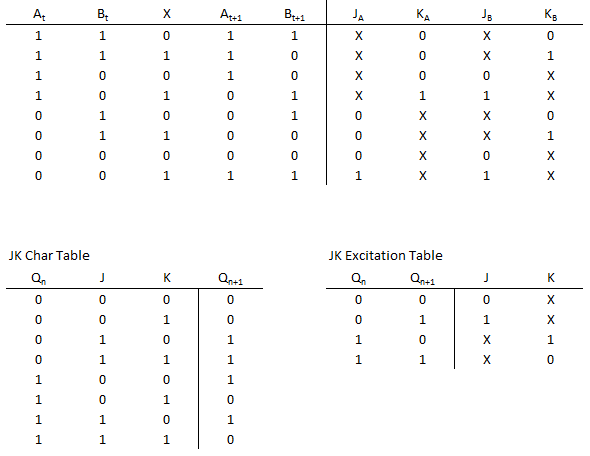
JK
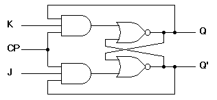
- Q is used as in input for the AND to prevent the race condition.
D
Designing a Sequential Circuit
This is best shown through an example, so we'll examine the 6 steps with a set example for this entire section.
- Description of circuit
- State Diagram
- State Table
- Excitation Table
- K-Maps
- Final Design
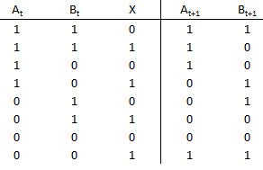
Description of Circuit
Let's make a 2-bit binary countdown. So that's 11, 10, 01, 00, and back to 11.
State Diagram
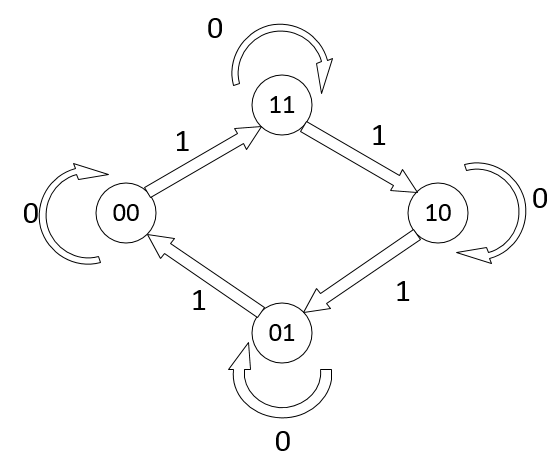
State Table
- List current states (one for each output bit)
- List inputs
- List next states
- Fill in based on State Diagram
Excitation Table
- Excitation Tables tell us what input is needed to move from one state to the next
- Each flip-flop has their own E-Table
- Built from Characteristic Tables (what inputs and current state result in next state)
- Decide on what kind of flip-flop you want to use
- Use one for each state bit
- Create new columns for each input of the flip flop for each state bit
- Reference E-Table for the flip-flop
- Fill in columns based on what state you're in and what you want next
K-Maps
- For each flip-flop input, create a K-Map
- X's from the E-Table can be either 0 or 1.
- Our goal is to make the largest, and fewest, loops
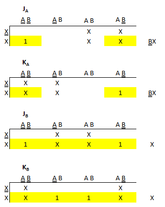
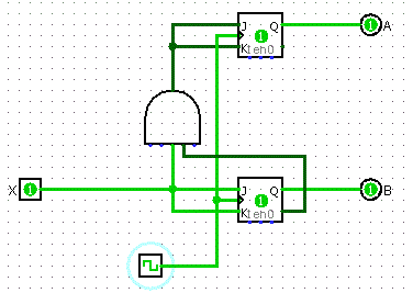
Final Design
- Take the results from the K-Maps to build your circuit
Buses and Memory
We need to tie in a ton of these sequential circuits to do actually useful things, but how do we do that? We can't have hundreds of thousands of separate wires running everywhere. We need to have the data run along a single main line.
Busses
- Invented to simplify organization and data flow
- Busses are a data path between many components
- A bus transfers data to and from components, on the same line!
- If multiple components try to talk at the same time, you get corrpted data on the bus
Bus Interface Unit
- Separate from the logic of the circuit.
- A simple switch to allow output or not.
Register
- A collection of many data lines.
- A 32 bit Register actually has 32 separate wires outputing.
- Displayed as a single line though.
- Larger registers allow larger throughput of data.
Memory
- Comprised of D Flip-Flops with a switch after its Q output.
- The switch is connected to a signal called Output Eabled.
- If OE, then Q will output to the data line, if not, the dataline is uneffected.
- The clock is connected to a signal called Write Enabled
- If WR is disabled, the flip-flop will not change, so it won't care about the data on the dataline.
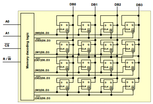
4 Bit Memory Unit
This is a 4-bit memory unit. It can output 4 data lines (4 bits). A single 4 bit of memory is stored horizontally, and 4 groups of 4-bits of data are stored vertically. Even though data line connects to every D input in a vertical line, the flop will only change if the clock is active. Likewise, the output from the flop will only affect the line if the output is enabled. Clock and Output cannot ever be both enabled.
- A0 and A1 select which horizontal line of D-flops will be enabled.
- There are 4 addresses, so we need 2 bits to address every memory location.
- CS is Chip Select. Means this chip is enabled for use (seen later)
- Read or Write. Enables the output, or enables the write respectively.
Memory Unit Sizes
- A memory unit can have N data lines in, and N data lines out.
- A memory unit can have M address lines.
- This is the actual capacity of the the memory unit.
- Memory is referenced as M x N, or M addresses by N data lines
- This is the number of bits each address stores.
Constructing Memory from Smaller Chips
Larger Memory can be constructed from smaller chips. We just have to make sure that the number of datalines are present as needed and have enough address lines (capacity) as needed.
- Can stack to increase capacity.
- Can stack to increase data lines.
- rows are called pages.
- We need to use extra bits to reference which page we want.
Paging
When large memory is constructed from smaller chips, we need a way to indicate which chips need to send/receive data from the bus. Pages are formed when memory is stacked to increase the number of addresses, not the number of data lines. Paging is used to select just enough chips to make use of all the data lines in the bus.
For example, 128KB x 16 memories built using 32KB x 8 chips. That's 2 chips per page (8 bits x 2 = 16 bits, as needed for the data line) and 21 pages. There are 2 chips per page, so each page is 215 * 2 = 216, and 217 / 216 = 21. This means 17 bits for address selection, 1 bit for page selection, and 1 bit for chip selection. The address will be sent to 2 chips to meet the 16 bit dataline. The page will be used to activate 2 chips via the chip selection.
- Chip Select is used for allowing only certain chips that are a part of a page to output data.
- This outputs fewer data bytes than the bus may allow.
- This is used to allow output to be made up of different addresses on different chips, and eventually end up with just one output.
- Offset Address is the address for each unique reference for each chip
- The page address is used externally, like the offset address.
- The chip select is used internally.
Microprocessor
Microprocessors have an associated memory system and use 2 busses to interact with it. An address bus and a data bus.
Addressability
Addressability means how the processor will access data, regardless of its data bus size. This only matters when
- Byte means the processor will access 1 byte at a time.
- Word means the processor will access 2 bytes at a time.
Concerning the memory unit
- The number of data lines must be filled by the memory unit.
- The outputs of each chip, and the number of data lines needed, determine the number of chips per page.
- Bits for Chip Selection are determined by how the processor is addressable.
- If the processor addresses 1 byte at a time, it needs to activate 1 chip every time.
- If the processor addresses 2 bytes at a time, it needs to activate 2 chips every time.
- The number of bits needed is determined by how many chips there are per page and how many chips need to be accessed at once.
- For byte addressing with 4-chip pages, that's 2 bits to access each 4 chips individually.
- For word addressing with 4-chip pages, that's 1 bit to access each 4 chips, 2 at a time.
- The number of pages you need depends on the number of address lines (total capacity) divided by the memory of the chips per page.
Address Space Partitioning
This is the act of creating address locations for your memory and having each bit mean something. You'll need A bits for chip selection, B bits for page selection, and then C bits for offset addressing.
- Every address line in the microprocessor must be used.
- Address Offset is the number of bits needed to address for each chip.
- Bits are set aside for chip select if needed.
- Then set aside bits for page selection.
How We Do
- Chips needed per page to fill data lines.
- Bytes per page = bytes per chip * number of chips per page.
- Bits for chip selection depending on processor addressing
- Total capacity = 2 to the number of address lines * bytes addressed.
- Number of pages = total capacity / bytes per page
Endian
Only concerns when byte/bit data is packed into larger capacities like longs or bytes.
- Big Endian, normal happy sequential data.
- Little Endian, weird messed-up reversed data.
Assembly Language
Every computer has a fundamental set of operations it can perform.
- Instruction Set codes are defined by a computer.
- Machine Language are 0s and 1s that reference memory locations and machine operations.
- Mnemonics are machine code instructions.
- Op-Code are also machine code instructions
- Assembler is a compiler that turns assmbly code (op-codes and mnemonics) into 0s and 1s.
- Pseudo Op-Code are codes that only the assembler understands. Make assmbly code easier to read
- Uses Labels just like the graphing calculator!
Keywords
- # is used to reference literal numbers, like #14 means the decimal number 14.
- $ is used to reference hexadecimal numbers and addresses
- Add a # prior to use a literal hex number, #$FF
- Just a $ means an address location
Our class is practicing with the 68k processor.
Components of the 68k processor
- Data Registers store up to 4 bytes of data. Referenced as D<number>, as in D0
- Data Registers are not memory, but something else.
- Address Registers store up to 4 bytes to refer to an addres location. These are pointers.
- Address Registers are used to access memory locations.
- ORG $address
ORG
MOVE
Moves some number of bytes from one location into another. The size is specified with either B, W, or L to mean Byte, Word, or Long respectively.
AND
Performs a bitwise AND between the two operators, storing the result in the last operator.
Register Direct Addressing
Even in c or C++, you can store data directly to a data register, which is even better and faster than RAM! Best used for data that will be accessed frequently.
Negative Numbers
Computers always work with signed numbers. To see how a computer stores negative numbers, see the Signed Bytes handbook entry.
Likewise, machine code cannot subtract numbers, it just uses add, but makes a number negative first.
Overflow
- Adding two positive numbers results in a negative number.
- Adding two negative numbers results in a positive number.
The result is out of range, so the computer results in an incorrect answer.
Status Register
A series of bits to check on the flags of errors. In 68k, it's XNZVC, and V=1 on overflow, C=1 when there is a carry.
Floating Point Numbers
Convert 3.8125 to binary! Two parts, integer and fractional part.
- Integer to binary part. 3 becomes 11
- Multiply fraction by 2.
- Write down the integer part, carry remainder.
- Repeat until no more fractional part.
- 0.8125 * 2 = 1.625
- 0.625 * 2 = 1.25
- 0.25 * 2= 0.5
- 0.5 * 2 = 1
- Result: 11 1101
Now we go back! Im, Im-1, ..., I1, I0.F1, F2, ..., Fn
I * 2m + I * 2m-1 + ... + I * 20 + F * 2-1 + F-2 + ... + F-n
What about irrational numbers that go on forever? 0.6 becomes 0.100110011001100.....
We have to just stop after some number of bits. Truncation is just dropping some bits. Rounding is better, but complicated.
How it's actually stored in computers
Two represetations. Fixed-point or floating-point.
Fixed Point
- Divide bits into 3 parts.
- Integer part - like above
- Fraction part as a single value. 3.625 becomes 0011 integer, and 0.625 becomes 1011--------------------------
Floating Point
- Divide bits into 3 parts.
- Sign (1 bit)
- Exponent (8 bits)
- Mantissa (23 bits)
- double has exponent with 11 bits, and mantissa with 52 bits.
Convert
- Convert decimal to binary. All parts. (Like above, multiply by 2)
- Normalize (only 1 digit in front of decimal, scientific form)
- Add 127 to exponent
- Mantissa is the one after the floating point in the normalized form
-3.8125
- -11.1101
- -1.11101*21
- Sign = 1
- Exponet bits = 1 + 127 (biased) = 128 = 10000000
- Mantissa bits: 111 0100 0000 0000 0000 0000
- Total: 1 100 0000 0 111 01 00 0000 0000 0000 0000 = 0xC0740000
We used biased exponents, because the exponent has 8 bits. Therefore, if we add 127 to the exponent, then there will never be an overflow problem.
Doubles have 64 bits. The only change to the rule is to add 1023 as an exponent bias, and not 127.
Stack
The general idea is to only use either post-increment or pre-decrement for accessing addresses. It's backwards in 68k. You set the start of the stack at some address A.
Push data using pre-decrement so that the address is decreased by one unit and the data is stored in this new address location. This way, data is never overwrittenon the stack.
Data is popped by using post-increment so that the address is referenced and used for something, then the address is incremented. This leaves the previous data intact (unless it was used to store data or something), but vulnerable to being overwritten by a push operation on the stack.
Memory and Cache
SRAM vs DRAM, static versus dynamic. SDRAM is just Syncrhonized DRAM.
SRAM is faster, more expensive because of more transistors, but its performance is used for cache.
DRAM is cheaper, uses a capacitor, but this means it has to keep refreshing to keep data, but this could mean a loss of data.
- Temporal localit means it will be referenced frequently
- Spatial locality nearby items tend to be referenced again soon/
- Block minimum unit of data
- Just some number of bytes.
- USually between 4 and 64 bytes, must be a power-of-2
- Hit data requested is in the cache (upper level)
- Means data doesn't have to be fetched from a lower level.
- We want to optimize hit-rate, reduce misses.
- Miss data requested is not in the cache (lower level)
- Effective Execution Time (EET), a way to benchmark hit rate.
Memory Heiarchy
- Memory closer to CPU is faster with lower capacity.
- Memory farther from CPI is slower but has higher capacity.
Cache
- May be multiple levels of cache. Lower levels are lest fast.
- For example, there can be word transfers from CPU and cache, but blocks of data are transfered if not in cache.
- Tag Register holds memory address and determines if there is a match
- Does not actually hold the address, but some value (mapping).
- Write Policy, change a data value in a cache
- Replacement Algorithm, what to replace when cache is full
- Cache Address, Is it a physical cache or a virtual cache?
- Line/Block Size, how many adjacent data should come together in a cache
- What is the optimal number of caches?
Effective Execution Time
- Hit Rate, precent of accesses found in cache
- Hit Time, time to access cache
- Miss Penality, time to replace block in cache with appropriate one (100x longer!!)
- EET = hit rate * hit time + miss rate * miss penalty
- Goal is to minimize EET
- Decrease miss rate (thus increase hit rate)
- Cannot just get rid of miss rate, because cache is too expensive to completely replace RAM
Mapping Function
- Maps a memory address to a cache tag
- Direct Mapping
- Associative Mapping
- Set Associative Mapping
- 4-way set associative cache is the most commonly used.
Direct Mapping
Suppose a main memory system has 32 byte capacity, byte-addressable, and cache has 8 byte capacity. A block has 2 bytes. One tag register corresponds to two bytes of cache memory.
Rearrange main memory as a number of columns (pages) so that each column (page) has the same size as the cache. Since cache is 8 bytes, each column is 8 bytes. This means there are 4 columns to use up all 32 bytes.
For example, we want memory at address 8 into the cache. Our rule is to map the 0
Binary, address 21 is 10101. The first two bits are the column number (column 2), next two are block number (2nd block), and last is the byte in the block (1st byte). Binary, address 8 is 01000. Column 1, block 0, byte 0.
- Divide address into tag, row, and offset bits
- Physical (RAM) Memory size: R bytes
- Direct-mapped cache size: C bytes
- The Cache block size: B bytes
- Coumns in a main memory: R / C = # tag bit is log2(R/C)
- Blocks in a cache memory: C / B = # row number bit is log2(C/B)
- Block size in a main memory: B = offset bit is log2(B)
- In our example...
- R = 32 = 25 (5 bits to represent every address)
- C = 8 bytes
- B = 2 bytes
- # columns = R / C = 25 / 23 = 22
- # of blocks = C / B = 23 / 21 = 22
- # offset bits = log2(21) = 1
- 2 bits for column, 2 bits for block, 1 for offset.
Determining if memory is in cache or not
- Go to the same block (row) in cache.
- Comapre the tag value in the tag register to the tag val you want.
- Equal means a hit, not-equal means a miss.
Problems
- Repeatedly accessing data of the same block, but from different pages causes a lot of miss penalties.
- There's no easy way to determine, in-code, if your cde will cause this problem.
Associatve Cache
The only difference is tha the number of columns is equal to the number of blocks.
- Rearrange the main memory based on the size of the block.
- # columns = L / K
- Bits per column = log2(# columns)
- This means there is no separation of tag and page, it's all just tag now.
- In our previous example with 5 bit addresses, this means the first 4 bits are for the tag, and the last is for offset.
Hit or Miss
- Since we don't have a block (row) anymore, we just have a tag and the tag-register.
- Search tag register for your address' tag ID. If found, hit!
- If tag not in register, then use an algorithm to write into cache.
Problems
- Search whole tag-register to find them, very slow.
- When tag-register is full, what should be removed (victim block)?
Set-Associative Cache
- N-Way Set Associtative Cache
- Divide the cache into multiple sets
- Each set contains N number of blocks
- Rearrange memory as number of columns so that each column (page) has the same number of blocks in a cache set.
Instead of rows mapping to one exact row in the cache (direct mapping), each block-row in a page (column) of memory maps to one set in the cache. When the cache asks for that data, it stores it in any available cache-block in the cache set.
- Memory size R
- N-way Set Associative Cache Size C
- Cache block size B
- # of columns in main memory: C / (R / N)
- # of sets in cache: (C / B) / N
Example with 32 byte system
- R = 32 bytes
- 2-way Set, with a cache C = 8 bytes
- Cache block size B = 2 bytes
- Pages = 32 / (8 / 2) = 8 = 23
- Sets = (8 / 2) / 2 = 2 = 21
- Offset bits = log2(2) = 1
Example
- Memory size with 2^14 bytes
- 2-way set
- Cache block size of 8 bytes
- Blocks in cache = 16
- ...
- Cache size = 16 * 8 = 128 = 27
- Bits for the offset = log2(8) = 3
- Number of sets = (27 / 23) / 21 = 23
- Bits for the set = 3
- Number of pages = 214 / (27 / 21) = 28
- or, 14 bits - 3 - 3 = 8
Finding Hit or Miss
Instead of just checking a certain row in the tag register for a tag value (direct mapping), we instead check set bits for the expected set. Then search the tag register in that set for the expected tag. If you find it, it's a hit!
Calculating Miss Penalty
This is a slightly complicated procedure that depends on how much data the processeor can read in from memory at once, and the time it takes to read in that data, how big a cache block is.
- Address Setup Time, some setup time to read
- Burst-Fetch Speed, the cycles it takes to get memory into cache
Example
- Address Setup = 5 cycles
- Burst-Fetch = 2 cycles
- 32 bit data bus, so 4 bytes in at once.
- Cache block that is 64 bytes big.
- We need 64 / 4 = 16 fetches to fill a cache block fully.
- Each fetch takes 2 cycles, so that's 16 * 2 = 32 cycles.
- Total: 5 + 32 = 37 cycles for a miss.
Cache Write Strats
Reading from cache is easy, but what if that cache data gets changed? We need to write to the main memory.
- A memory cell that has an updated value still in cache is called a Dirty Cell.
- Write-Through cache. Data is written to the cache and main memory at the same time.
- Write-Back cache.
- Data is held until bus activity allows the data to be written without interrupting other operations.
- May also wait until has an entire block of data to be written.
- The write-back of the data is called a post-write.
- Write-Around cache
- Non-cached data is immeditaely writen to memory (do not go through cache)
- Or, if there is a cache block available with no corresponding dirty memory cells, it may store the data in that cache first.
Performance
- Execution time = (execution cycles + stall cycles) * cycle time
- Stall cycles = # of instructions * miss ratio * miss penalty
- Two ways to improve performance:
- Decrease miss rate, increase block size.
- Decrease miss penalty.
- Multiple Caches (see below)
- Multiple levels of cache. At each level, you can make optimizations.
We can also split cache into two parts! Instruction cache and data cache! There is more spatial locality in instructions than data.
Virtual Memory
This concept works in tagent with OS and Hardware. When you use addresses in C++ or Java, you're using Virtual Addresses, not physical addresses. Embeded systems don't usually have this feature.
- Maps lower memory to upper memory.
- Upper memory is like RAM.
- Lower memory is like a hard drive.
- Allows programs to pretend that they have limitless memory to run and store data.
- It uses hard disks, with much higher storage, to be used like RAM.
- Any page in a virtual memory can be mapped to any page on phyiscal memory.
- You can directly translate the address in VM to physical memory using a page table.
- Demand-paged virtual memory, OS loads pages into RAM
Partitions
- Virtual Page Number
- Byte Offset
Pages
- Blocks of memory that can map between upper and lower memory.
- Only pages that are needed by CPU are loaded into RAM.
- Page number is translated into a frame number in RAM.
- Frame is the exact same as Page, but "Frame" is the term used in RAM
Page Map
This is a mapping function that maps virtual to physical memory.
- Virtual Page Number, the index in the page table.
- Page Frame Number, the Frame number in RAM.
- Validity Bit, whether or not the page is currently in RAM.
- Dirty Bit, If the program has written to the page.
- Security Bit, Which users can access the page (Linux CHMOD).
Think of the mapping like a 2D array (2 columns). There's a slot for each Page (VM), the index directly corresponds to the Page number. The first column stores the Frame number (RAM page number) for that VM Page. The second column stores the validity bit. If v-bit is 0, then the Page is not loaded, and the first column holds junk data. If the v-bit is 1, then the Page is loaded at the Frame number indicated in the first column.
Example
- Virtual memory is 32 bytes
- RAM is 8 bytes
- 1 Page is 2 bytes
- Pages = V / P = 32 / 2 = 16
- Frames = R / P = 8 / 2 = 4
- Map the Page into one of the 4 Frames.
Map 0x0404 from VM to RAM
- VM = 13 bits
- RAM = 12 bits
- Pages = 8, 3 bits
- Frames = 4, 2 bits
- 0x0404 = 0000 0100 0000 0100
- Page = 1
- Table at index 1 is valid
- Frame number at index 1 is 3
- Frame = 3
Page-Table Base Register
This is a pointer to the beginning of the table. The OS can modify the page table directly. In theory, main memory (non-cached) accesses could take twice as long because the page table must be accessed first.
Translation Looaside Buffer (TLB)
Modern processesors use this form instead. This holds the same information of the page table, but in cache! This means it cannot be nearly as large. TLB only saves information for the most recently accessed pages to accomidate for this.
Virtual Paging Process
- CPU Generates an Effective Address
- TLB takes EA
- TLB has valid Frame, if so end and generate RAM address
- Scan page table in main memory
- Page in physical memory? If so, update TLB and generate RAM address
- Page fault exception, OS loads data from hard drive to RAM.
Replacement Policy
- Least Recently Used(LRU)
- Evicts the fram that has been unused for a long while.
- Complex, have to maintain history for each block, slows down cache.
- First-In First-Out
- Throw away the frame that has been in cache the longest.
- Random
Least Recently Used
An algorithm to track Memory blocks or pages and track how recently they were used.
Imagine a queue, holding the number of last Frame/Page used. The front of the queue is the least recently used, the back is the most recently used. If a Page, already in the queue, is used again, it gets out of line and sent to the back. New Page entries cause the front of the queue to be removed completely, with the new Page going to the back.
Example
- R = 256KB = 218
- P = 64KB = 216
- V = 1MB = 220
- 2-entry TLB
Virtual Breakdown
- 20 bits for address
- 16 bits for offset (size of a page)
- 4 bits for page
Physical Breakdown
- 18 bits for address
- 16 bits for offset
- 2 bits for Frame.
Convert 0xA4620 from Vritual to Physical address
- 1010 0100 0110 0010 0000
- 1010 = Page = A
- Lookup A in page table.
- Check TLB first
- Now check Page Table
- If still not valid, push data from disk to memory.
- Update LRU tables.
Putting Memory Together
We're ultimately trying to read data only from the cache. So all of the annoyances we did creating physical and virtual memory, page tables and LRU, is to ultimately generate a physical address. With that physical address, we're gonna futher manipulate it to check the cache for the data. If it's there, great! If not, let's upload it.
Cotinuing example from above
- Direct Mapped L1 Cache Size = 4KB with 256 Bytes/Block
- 2-way Set Associative L2 Cache Size = 16KB with 1024 Bytes/Block
Breakdown Physical Address to L1 Cache Addres
- Offset = 8 bits (256 Bytes/Block)
- Blocks per Cache = 4KB / 256 = 24, 4 bits
- Therefore, 6 bits for Tag (18 - 6 - 4)
Breakdown Physical Address to L2 Cache Address
- Offset = 10 bits (1024 Bytes/Block)
- Sets = (16KB / 1024) / 2 = 8, 3 bits
- Therefore, 5 bits for Tag (18 - 10 - 3)
Syllabus
- Dr. Yang Peng
Software
- Logisim (Logic/Circuit)
- Easy68k (Simulator for Assembly language programming)
- 68000 Programmer's Refernce Manual (Processor Manual)
- 68000 Family Assembly Language
Project
- 2 to 3 players
- Develop a popular computer architecture
- Covers 25-30% of grade
Lab
- Uses your own laptop
- Install needed software Done all in class